3.2、 Analysis of Commutation Process
The commutation process of the parallel inverter circuit is shown in Figure 5:
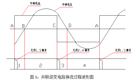
Due to the oscillation characteristic of the circuit, after oscillation is established, if none of the four bridge arms is triggered, the oscillating voltage and current will continue under the premise of ignoring circuit loss. In actual conditions considering circuit loss, the oscillation will gradually decay. When analyzing one working cycle of the circuit, the influence of damped oscillation can be ignored, and the circuit can be regarded as a complete oscillation state.
When there is oscillating voltage (current) on the load, SCR components must be triggered at proper time to ensure the normal operation of the parallel inverter circuit; triggering SCR components at improper time has a high probability of causing short-circuit fault.
The following is the analysis of the working state of Figure 5:
When the electrical parameters of Figure 5 match the circuit of Figure 4, the positive voltage direction is defined as when the left side of the load circuit is positive polarity, and the positive current direction is defined as when current flows from the left side into the load circuit.
In the AB interval, the intermediate frequency voltage is negative, which means SCR1 and 3 are subjected to forward voltage. Therefore, when components 1 and 3 are triggered at point A, components 1 and 3 conduct. Until point B, the intermediate frequency voltage becomes positive. Under the conducting state of SCR1, the DC power supply transmits energy to the load circuit through the filter inductor; after point B, SCR2 and 4 are subjected to forward voltage. Therefore, when SCR2 and 4 are triggered at point C, they meet the conducting condition, and the current commutates to SCR2 and 4.
The electrical angle covered by AB interval and CD interval is called the commutation angle. During the commutation angle, the transition process that one pair of components conducts and the other pair turns off is completed. After triggering SCR1 and 3 at point A, SCR1 and 3 conduct, and the current of SCR2 and 4 gradually decreases to zero (limited by L2 and L4, it cannot drop to zero immediately), which takes about 10us. The subsequent period is the time required for SCR2 and 4 to restore blocking capability, commonly known as "turn-off time" (the turn-off time of current components is less than 30us). If the operating frequency of the inverter is 2000Hz and the commutation angle is 30° (the total angle of AB interval and CD interval), the interval time is 41.7us ((1000000/2000)*30/360=41.66). It can be seen that the commutation time of the circuit is greater than the sum of the current decay time and the turn-off time of the components, so the components can be turned off reliably. If the commutation angle is reduced so that the commutation time of the circuit is less than the sum of the current decay time and turn-off time of the components, SCR2 and 4 will conduct again before they recover blocking capability and are subjected to forward voltage again, causing short circuit of the inverter bridge.
The commutation angle is the phase difference between the load voltage and the load current, that is, the power factor angle Φ of the load circuit.
The above analysis shows that an excessively small commutation angle cannot ensure normal commutation of SCR components. The existence of the commutation angle makes the load current lead the
Where: Pd---DC power
Ud---Average DC voltage
Id---Average DC current
Ia is the root-mean-square value of the fundamental wave of the square wave current. According to Fourier series decomposition, the relationship is Ia=0.9Id, and Pa=Pd, therefore:
Ua=1.1Ud/cosΦ (5)
Equation (5) is the direct basis for measuring the commutation state of a parallel inverter circuit. When Φ varies within the range of 25º to 45º, the value of Ua/Ud ranges from 1.214 to 1.56. In actual debugging, it is safe and reliable to control the ratio of medium-frequency voltage to DC voltage within the range of 1.2 to 1.5.